
Checklist for Inspecting Solder Joints
[ Back to Mechanical Keyboards 101 ]When building custom mechanical keyboards, inspecting solder joints is essential for ensuring reliable performance. Defective solder joints, like cold solder joints or solder bridges, can cause electrical failures, intermittent connections, or even damage to the PCB. Here's what you need to know:
Key Takeaways:
- Good Solder Joints: Smooth, shiny for leaded solder; satin-like for lead-free. Look for a concave shape with proper wetting.
- Common Defects: Cold joints (dull, grainy), solder bridges (shorts between pads), tombstoning (components standing upright), and solder balls (can cause shorts).
- Inspection Tools: Use magnification (10x-20x for fine details), proper lighting (1,000 lux), and a multimeter for electrical checks.
- Advanced Techniques: Automated Optical Inspection (AOI) for surface defects and X-ray for hidden issues like voids or internal solder bridging.
Pro Tips:
- Clean the PCB with isopropyl alcohol before inspecting.
- Use fresh flux for rework and avoid overheating components.
- Document all defects clearly for efficient repairs.
Thorough inspection ensures your keyboard performs reliably and lasts over time. The process combines visual checks, advanced tools, and careful rework when needed.
How to Spot a Bad Solder Joint
sbb-itb-3cb9615
Visual Inspection Checklist
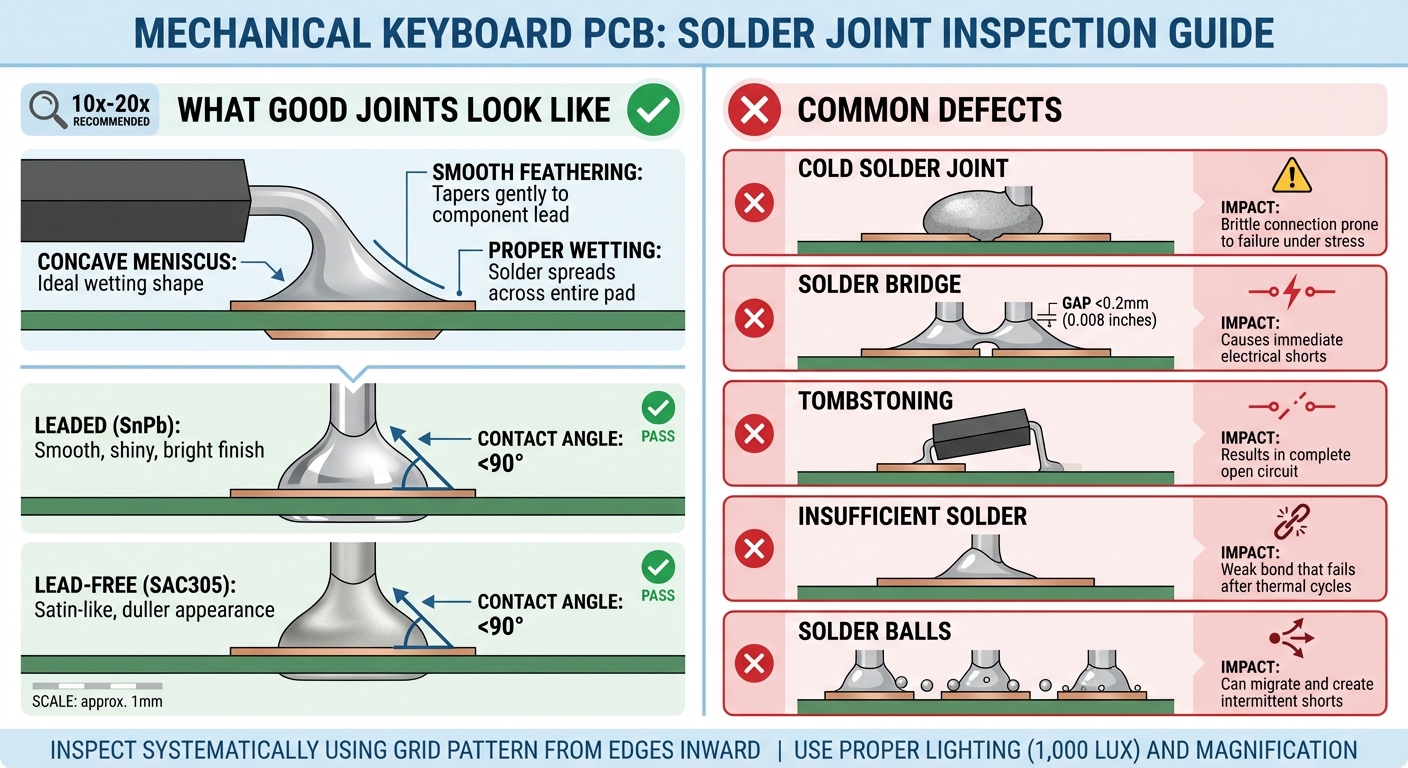
Visual Guide to Solder Joint Defects vs Good Joints
Once your PCB is clean and tools are ready, inspect the board systematically. A grid pattern, starting from the edges and moving inward, ensures no area is overlooked.
What Good Solder Joints Look Like
A well-soldered joint has distinct visual traits. For leaded (SnPb) solder, you should see a smooth, shiny, and bright finish. The solder should form a concave meniscus, smoothly feathering out onto both the pad and the component lead. This shape is a sign of proper wetting, which happens when the contact angle is less than 90 degrees.
"Proper wetting creates a concave meniscus (fillet). A cold joint often looks convex, bulbous, or 'balled up' because the solder's surface tension exceeded the adhesive force to the pad." - JLCPCB
For lead-free solders like SAC305, the finish is naturally duller. However, don't confuse this satin-like appearance with a flaw. Uniformity is key - look for a smooth surface without crusty or grainy textures. The solder should flow seamlessly onto the pad, with no gaps or visible cracks at the interface. For through-hole components, confirm that the leads are trimmed properly and that solder has wetted both the lead and the barrel of the hole. Ground connections deserve extra attention - thermal relief "spokes" are essential because large copper planes can act as heat sinks, increasing the risk of cold joints during soldering.
Common Visual Defects
Now that you know what to look for in a good joint, let’s address common defects and their telltale signs:
- Cold solder joints: These appear dull, grainy, or rough instead of smooth. Their convex or bulbous shape indicates poor bonding. Cold joints are brittle and prone to failure during thermal cycling.
- Solder bridges: These are unintended connections between adjacent pads, often found in fine-pitch packages where pad gaps are smaller than 0.008 inches (0.2 mm). They can be hard to spot but are highly damaging to circuit functionality.
"These bridges are invisible to the naked eye but lethal to circuit function." - JLCPCB
- Tombstoning: This occurs when one end of a small surface-mount component lifts off its pad, leaving the component standing upright and creating an open circuit.
- Solder balls: These tiny metallic beads near joints might seem harmless but can migrate between traces during thermal cycling or vibration, eventually causing shorts.
- Insufficient solder: A fillet that's too small signals a weak mechanical bond, which can fail after repeated thermal cycles.
- Excessive solder: This buries the lead in a large mass, making it impossible to visually verify the connection's quality.
- Component misalignment: Parts that shift off-center during reflow are another red flag requiring attention.
| Defect Type | Indicator | Why It Matters |
|---|---|---|
| Cold Joint | Dull, grainy surface; convex or bulbous shape | Brittle connection prone to failure under stress |
| Solder Bridge | Unintentional connection between pads | Causes immediate electrical shorts |
| Tombstoning | Component standing vertically on one pad | Results in a complete open circuit |
| Insufficient Solder | Thin, small fillet | Weak bond that fails after thermal cycles |
| Solder Balls | Tiny metallic beads near joints | Can migrate and create intermittent shorts |
This thorough visual inspection sets the stage for more advanced techniques to ensure every solder joint is reliable and up to standard.
Advanced Inspection Techniques
Visual inspection can catch surface defects, but hidden flaws need more sophisticated methods. Components like Ball Grid Arrays (BGAs), Chip Scale Packages (CSPs), and Quad Flat No-lead (QFN) hide their solder joints beneath their bodies, making advanced techniques essential to ensure quality and reliability.
Automated Optical Inspection (AOI)
AOI systems rely on high-resolution CCD or CMOS cameras to capture detailed PCB images and compare them to a "Golden Board" reference or CAD specifications. The process involves several steps: capturing images with LED lighting, analyzing data with algorithms, classifying defects by severity (Critical, Major, Minor, or Pass), and generating reports with defect coordinates and trends.
These systems are incredibly efficient, inspecting boards up to 50 times faster than manual methods while maintaining detection accuracy above 99.5%. They can detect solder bridges as small as 50 μm, and unlike human inspectors, they never need a break.
2D AOI is great for spotting surface defects, but 3D AOI takes it further by using laser scanning to measure height and volume. This makes it ideal for identifying coplanarity issues and inspecting hidden areas like BGAs and QFNs, where lifted leads would otherwise go unnoticed. Implementing AOI early - at the solder paste stage - can cut overall defect rates by up to 50% in high-volume production of 75% mechanical keyboards. This is especially critical since 70% of PCB assembly defects stem from improper solder paste application.
X-Ray Inspection for Hidden Defects
AOI is excellent for surface-level inspections, but X-ray technology is the go-to for uncovering hidden voids and internal defects. When solder joints are concealed beneath component bodies, X-ray inspection becomes a necessity. This method identifies issues like voids (air or gas pockets trapped in solder), Head-in-Pillow (HiP) defects (failure of the solder ball and paste to merge), and internal solder bridging that optical methods might miss.
For compliance with IPC Class 2 and Class 3 standards, void areas in a single BGA solder ball must not exceed 25% of the total ball area, and the largest void must stay below 20% to avoid stress concentration. While 2D X-rays can calculate total void percentages, they may miss HiP defects due to vertical overlap. Using 2.5D scans (angled 45–70°) or 3D laminography provides a clearer view, revealing the "snowman" separation signature characteristic of HiP defects.
"Head-in-Pillow (HiP)... is generally not acceptable. It appears as a distinct separation or lack of coalescence between the solder ball and the paste." - APTPCB
It’s best to inspect before applying underfill, as this material alters contrast and complicates void detection. Pay close attention to interfacial voids at the pad/solder connection - these are high-risk areas that can lead to brittle fractures, even if the total void size is within acceptable limits.
Testing Solderability and Strength
Imaging techniques are crucial, but physical tests are equally important for confirming the mechanical strength of solder joints. The Wetting Balance Test measures the vertical forces on a specimen immersed in molten solder over time. A steeper slope on the wetting curve indicates faster solder spread and better solderability. The curve crossing zero marks the moment solder wetting begins.
"Solderability refers to the ability of a metal surface (component lead, termination, PCB pad) to be wetted by molten solder." - Wevolver
The Dip and Look Test evaluates solder coverage, requiring at least 95% coverage for component leads and 80% for pads under 10x–20x magnification. Before testing, steam aging (8 hours at 93°C) simulates long-term storage and environmental wear, ensuring results reflect actual conditions.
Troubleshooting and Documentation
After identifying issues through advanced inspection, accurate documentation and timely rework are key to maintaining quality.
Recording Defects and Observations
Keeping a detailed record of defects ensures alignment with IPC-A-610 standards and streamlines the rework process. Each defect must be logged thoroughly so others can locate, understand, and address the issue without confusion.
Evaluate solder joints based on IPC-A-610 standards and classify them into one of four categories: Target (perfect), Acceptable (functional but not visually ideal), Process Indicator (a warning of potential process issues that doesn’t impact functionality), or Defect (requires rework or scrapping). This system eliminates subjectivity - quality is defined by clear, measurable criteria.
Mark the defect’s location using arrows or stickers and record its reference designator (e.g., "U12 – Bridging"). Include the board’s serial number and the IPC Class (1, 2, or 3) being applied. Remember, moving from Class 2 to Class 3 typically increases assembly costs by 15% to 30% due to the stricter criteria. Use either a digital quality management system (QMS) or physical documentation to maintain a permanent record. Additionally, every manual repair must be verified and logged to close the defect entry.
"Quality is not a subjective feeling; it is a defined set of visual and mechanical standards." - APTPCB
Rework should only address actual defects. Unnecessary reheating can introduce heat stress, which may reduce the long-term reliability of the board more than any cosmetic imperfection.
How to Rework Defective Joints
Once defects are documented, follow these steps to rework faulty joints effectively.
The primary goal of rework is precision and speed - apply heat quickly, fix the issue, and move on to minimize stress on surrounding components. Always follow ESD precautions.
Before reheating, apply fresh flux. The original flux burns off during the initial soldering, and reheating without flux means working with oxidized metal, which won’t wet properly. Clean any dirty or sooty joints with a cotton bud dipped in isopropyl alcohol before proceeding.
For solder removal, use a desoldering braid of the correct size. Place it over the solder, and remove both the iron and braid simultaneously at a 45° angle to prevent solder from reattaching to the board. Avoid dragging the wick across pads, as this can scratch the copper surface. For through-hole components, a solder sucker is often faster, while a hot air station is ideal for BGAs and QFNs, as it provides even heating across multiple leads.
If a pad begins to lift during rework, stop immediately - this indicates structural damage. Similarly, if ground connections frequently cause defects, check the design for thermal relief "spokes." These features prevent the copper plane from acting as a heat sink, which can make soldering more difficult.
Conclusion
Review of the Inspection Process
The inspection process for custom keyboard builds is crucial to ensuring reliable performance. By combining visual inspection, circuit testing, and X-ray inspection, you can thoroughly identify defects that might compromise the board's functionality. Visual checks catch surface issues like solder bridges or misaligned components, while circuit testing verifies continuity and resistance. For hidden flaws, especially under BGAs or other bottom-termination components, X-ray inspection uncovers internal voids that visual methods simply can’t detect.
A three-tier inspection approach ensures no detail is overlooked. Pay attention to solder joints - look for a concave, "volcano"-shaped fillet with smooth tapering onto the pad. Keep in mind that lead-free solder naturally looks duller than leaded solder. Properly formed joints should show low resistance, while defective ones will have higher resistance. Refer back to earlier guidelines for magnification levels to ensure precision.
"PCB visual inspection is the front line in preventing defects, catching issues early in fabrication and upon assembly."
– Xiaoji Lee, FC PCBA
While Automated Optical Inspection (AOI) is a powerful tool, manual inspection remains the go-to standard for custom keyboard builds and prototypes. With the right magnification tools and a trained eye, you can spot issues that machines might miss.
Final Tips
To wrap things up, here are some essential tips for rework and design considerations. Custom keyboards endure unique challenges, like constant typing vibrations, thermal cycling, and mechanical stress from switch actuation. Even if a cold joint passes initial tests, it could fail over time.
- Always use fresh flux during rework. Flux from the initial soldering burns off, and reheating without new flux means working with oxidized metal that won’t bond properly.
- Use the "wiggle test" to troubleshoot. If resistance changes when you gently press a component, you’ve likely found a cold joint.
- For PCBs with large ground planes, include thermal relief spokes in your design. Without them, large copper areas can prevent the board from reaching the 473°F peak reflow temperature needed for lead-free solder like SAC305.
- Maintain the solder above its liquidus temperature for 45 to 90 seconds to form a strong Intermetallic Compound (IMC) layer. Skipping this step can lead to weak, brittle joints.
Whether you're assembling your first custom keyboard or your hundredth, attention to detail during inspection and rework makes all the difference. Carefully examine each solder joint, document your findings, and prioritize quality over speed. This disciplined approach ensures your builds are reliable and stand the test of time.
FAQs
How can I tell a cold joint from normal lead-free solder?
A cold solder joint usually stands out with its dull, rough, or grainy appearance. It might also have visible cracks or uneven surfaces, indicating weak bonding between the solder and the component. On the other hand, a proper lead-free solder joint should look smooth, shiny, and well-formed. While lead-free solder is naturally less shiny compared to traditional tin-lead solder, it should still maintain a consistent and smooth finish. Visual inspection plays a crucial role in identifying these differences.
What’s the fastest way to find tiny solder bridges on a keyboard PCB?
To efficiently locate small solder bridges on a keyboard PCB, start by visually inspecting the board with a magnifying glass or microscope. Look closely for excess solder that might be connecting adjacent pads or pins. For a more precise check, use a multimeter to test for unintended electrical connections between pads. By combining these techniques, you can reliably detect even the tiniest solder bridges, including those that might not be immediately visible.
What multimeter checks should I run before powering the PCB?
Before turning on your PCB, grab a multimeter to double-check everything is functioning as it should. Start by testing continuity on key traces and connections to ensure there aren’t any broken paths or cold solder joints. Next, confirm there are no shorts between the power and ground lines. Also, take a moment to inspect components like diodes and switches to verify they’re properly connected and operating as intended. These precautions can catch potential problems that might lead to damage when you power up the board.