
Broken PCB traces can render your keyboard useless, but they’re often repairable with the right tools and techniques. Whether caused by spills, physical stress, or heat damage, fixing broken traces involves identifying the damage, repairing the electrical path, and securing the repair for long-term use.
Key Steps to Fix PCB Traces:
-
Identify the Damage:
- Clean the PCB with isopropyl alcohol.
- Inspect visually using magnification tools.
- Use a multimeter in continuity mode to locate breaks.
-
Gather Tools:
- Soldering iron, solder wire, flux, and desoldering wick.
- Jumper wires (30 AWG recommended), tweezers, and wire strippers.
- Cleaning supplies like isopropyl alcohol and flux remover.
- Magnification tools, Kapton tape, and epoxy for insulation.
-
Repair Methods:
- Wire Jumper Method: Best for larger breaks or high-current traces.
- Conductive Ink: Ideal for small cracks or low-current traces.
- Solder Blob Bridge: Suitable for minor gaps or hairline cracks.
-
Test and Insulate:
- Use a multimeter to confirm continuity and ensure no shorts.
- Apply epoxy or overcoat to protect the repair.
Fixing PCB traces saves money and extends the life of your keyboard. With careful preparation and testing, you can restore functionality and avoid costly replacements.
Repairing Damaged / Broken PCB Traces || Soldering Tutorial
sbb-itb-3cb9615
How to Identify Broken PCB Traces
Before diving into repairs, it's crucial to locate the damaged trace. This can be done using a combination of visual and electrical tests, which provide a solid foundation for the repair steps discussed later.
Visual Inspection Techniques
Start by cleaning the PCB with isopropyl alcohol and a soft brush. Once the board is clean, examine the traces under magnification tools like a jeweler's loupe, magnifying glass, or stereo microscope. This process helps detect even the tiniest cracks, as small as 0.1 mm.
Thermal damage often appears as burnt or charred sections, or even areas where copper has been vaporized due to overcurrent or short circuits. On the other hand, chemical damage shows up as greenish or crusty residue, typically caused by oxidation from moisture or battery electrolyte leaks. Focus on high-stress areas like solder joints, vias, and around batteries, as these are common trouble spots.
If you suspect damage beneath the solder mask (the protective layer over the copper), carefully scrape away the mask using a scalpel or scratch brush. This can expose micro-fractures that aren’t visible otherwise.
Once you've visually identified potential issues, confirm your findings with electrical testing.
Using a Multimeter for Continuity Testing
While visual inspection is helpful, it doesn’t catch everything. To test trace continuity, set your multimeter to continuity mode. Place one probe at the trace's starting pad and the other at its destination pad. If the multimeter beeps, the trace is intact. If it doesn’t, there's a complete break in the trace.
"A multimeter continuity test confirms trace integrity: open-loop readings indicate complete breaks, while abnormally high resistance suggests partial damage." - Hilelectronic
If the multimeter shows an OL (open-loop) reading, this confirms a full break in the trace. However, if you get a resistance reading instead of a beep, compare it to a similar, functional trace on the same board. Higher-than-normal resistance could point to partial damage, such as hairline cracks or corrosion. Always test again after making repairs and before applying any protective coatings to ensure the trace is fully restored.
Tools and Materials Needed
Once you've pinpointed the damaged trace, it's time to gather the tools you'll need for a precise repair. Here's a breakdown of the essential equipment for fixing a broken PCB trace.
Basic Tools for PCB Repairs
Start with a temperature-controlled soldering iron equipped with a fine conical or chisel tip. Precision is key - too much heat can destroy thin copper conductors or damage the board's substrate. You'll also need solder wire and flux to form strong electrical bonds, as well as a desoldering wick (also called braid) to remove excess solder and ensure a clean working surface.
For repairing the trace, use jumper wire of the correct gauge, such as #34 AWG for 0.010" traces or #26 AWG for 0.082" traces. Choosing the right diameter ensures the wire can handle the current without overheating. Pair this with precision tweezers for handling small wires and wire strippers with shear cutters to strip insulation and cut wires to precise lengths.
To expose the damaged trace, a precision knife or a rotary tool with grinding bits will come in handy. A rotary tool, especially one with speeds up to 40,000 RPM, allows for better control when scraping away the solder mask, minimizing the risk of cutting through the copper layer. You'll also need cleaning supplies like isopropyl alcohol wipes, lint-free pads, and flux remover pens to eliminate contaminants before soldering.
A digital multimeter is indispensable for checking continuity at each step and ensuring the resistance values match those of nearby functional traces. Magnification tools, such as a magnifying glass or microscope, can help you work with precision and avoid accidental bridging between traces.
For securing the repair, have polyamide (Kapton) tape on hand to hold jumper wires in place during soldering. Use two-part epoxy or adhesive wire dots to permanently bond wires to the board. To finish, apply an overcoat pen or epoxy coating (like CircuitWorks Epoxy Overcoat) to insulate and protect the repaired area. You can even tint the coating to match the board's original color - green, blue, or red - for a polished look.
Safety Equipment
Safety should always come first when working on PCB repairs. Heat, sharp tools, and delicate electronics can pose risks, so proper precautions are essential. Use heat shields - either aluminized shields or high-temperature tape - to protect nearby components like ICs, capacitors, or plastic connectors from heat damage during soldering.
ESD-safe equipment is a must when handling circuit boards. Wear an anti-static wrist strap connected to a grounded surface, and work on an ESD-safe mat to avoid static damage. Store your PCB in ESD-safe cases or trays when you're not actively working on it. Static discharge can harm sensitive components, even if the damage isn't immediately visible.
Protect yourself with safety glasses to shield your eyes from solder splatter and flux fumes. Heat-resistant gloves can prevent burns when handling hot parts or boards. Lastly, ensure your workspace is well-ventilated, as solder flux releases fumes that can be harmful if inhaled over time.
Step-by-Step PCB Trace Repair Methods
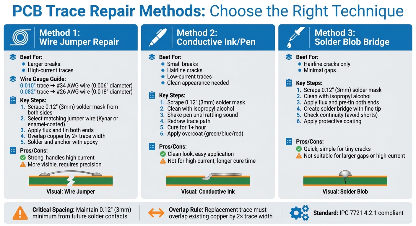
PCB Trace Repair Methods Comparison Guide
Choose the repair method that matches the type and extent of trace damage. Each approach has its advantages - wire jumpers are ideal for high-current traces, conductive ink offers a quick and clean solution for small breaks, and solder bridges are effective for tiny cracks with minimal gaps.
Method 1: Wire Jumper Repair
Start by removing the damaged trace and scraping off about 0.12" (3mm) of solder mask from both sides to expose the copper. Use a hand-held rotary tool with a grinding bit to carefully scrape the mask away, revealing bright copper. Clean the area thoroughly with an isopropyl alcohol wipe.
Select a jumper wire that matches the width of the damaged trace. For example, use #34 AWG wire (0.006" or 0.15mm diameter) for a 0.010" (0.25mm) trace, or #26 AWG wire (0.018" or 0.46mm diameter) for a 0.082" (2.08mm) trace. Kynar or enamel-coated solid wire is recommended, as it provides the necessary current-carrying capacity.
Apply flux to both the exposed trace ends and the stripped ends of the jumper wire, then tin them with solder. Position the jumper wire so it overlaps the exposed copper by at least twice the width of the trace. This overlap ensures a strong electrical connection. Solder the wire to both ends of the trace, keeping your work at least 0.12" (3mm) away from other components to avoid accidental reflow. Once the connection is secure, anchor the wire to the PCB with two-part epoxy or adhesive tape dots for added stability.
Method 2: Conductive Ink or Pen Repair
This method is ideal for small breaks or hairline cracks, especially when maintaining a neat appearance is important. Begin by scraping off 0.12" (3mm) of solder mask on both sides of the damaged trace to expose the copper. Clean the exposed area with an isopropyl alcohol wipe.
Shake the conductive ink pen until the particles are properly mixed (you should hear a rattling sound). Press the pen tip to the PCB and gently squeeze the barrel to dispense the ink. Carefully redraw the broken electrical path, allowing the ink to bridge the gap and restore the circuit.
Let the ink cure for at least one hour before handling the repair. Once cured, use an overcoat pen or epoxy to insulate the repair and protect it from oxidation. Overcoat pens are available in colors like green, blue, or red to match the original solder mask, helping the repair blend in seamlessly.
Method 3: Solder Blob Bridge
Solder bridges are best for repairing hairline cracks. For larger gaps or high-current traces, wire jumpers are a better choice. Begin by scraping off the solder mask to expose about 0.12" (3mm) of copper on both sides of the break. Use a precision knife or fiberglass pen for this step.
Clean the exposed copper with isopropyl alcohol, then apply flux and pre-tin both ends of the trace with solder. Using a temperature-controlled soldering iron with a fine tip, carefully create a solder bridge to span the gap. Take care to avoid accidentally bridging adjacent traces.
Once the bridge is complete, check continuity with a multimeter to ensure the electrical connection is restored and no shorts are present. To protect the repair, apply a liquid solder mask, UV-curable coating, or epoxy overcoat to shield the exposed copper from oxidation and environmental damage. This step ensures the repair remains durable over time.
Securing and Insulating the Repair
After fixing the trace, the next step is to secure and insulate the repair to ensure it stays functional over time.
Using Kapton Tape or Epoxy
Properly securing the repair is crucial. Without insulation, the repair might shift out of place or become corroded.
Kapton tape is a handy tool for temporary support during the repair process. It can hold jumper wires steady while soldering and protect surrounding components when applying epoxy. Keep the tape positioned away from the solder joint to avoid interference. Once the solder joint has cooled, carefully remove the tape before applying any final protective coating.
For a more permanent solution, an epoxy overcoat creates a durable shield. Follow the mixing instructions for the epoxy and apply it with precision using a pick. To achieve an even coat, use a lint-free foam swab to spread it, ensuring the trace is fully encapsulated. If you're short on time, acrylic overcoat pens are a quicker option. These pens cure faster and are suitable for areas with low heat exposure, but they might not handle high soldering temperatures as effectively as epoxy.
Before applying any coating, clean the area with isopropyl alcohol to remove flux residues and ensure the coating adheres properly.
Once insulated, the repair is ready for durability testing.
Ensuring Long-Term Stability
After insulating the repair, it's essential to confirm its stability and functionality. Use a multimeter to check continuity and resistance, ensuring the repair is solid.
If you're heat-curing epoxy, double-check that nearby components can handle the curing temperatures to avoid accidental damage. For environments with high moisture levels, applying a conformal coating over the repair area can help guard against corrosion over time.
To meet professional standards, such as IPC 7721 4.2.1, an overcoat is required to ensure reliability. Make sure the replacement trace overlaps the existing conductive surface by at least twice its width. Additionally, maintain a minimum gap of 0.12" (3 mm) from any contacts that might be soldered in the future. This prevents unintentional reflow during future maintenance tasks.
Testing the Repair
Once the repair has cured, it's time to ensure everything is functioning as it should. Using a multimeter to check conductivity and device functionality is a critical step to confirm the repair is solid and reliable.
Multimeter Testing
Start by setting your multimeter to continuity mode. Touch the probes together to verify the device is working - this should result in a reading near 0Ω and an audible beep. This step ensures your multimeter is ready before testing the repaired board.
For the test itself, place the probes on exposed copper at both ends of the repaired trace. Make sure the probes are in contact with the bare metal, not the solder mask, as this could give a false "OL" (open line) reading. A successful repair will result in an immediate beep and a resistance reading close to 0Ω. If the multimeter shows "OL" or doesn’t beep, the break hasn’t been bridged. A beep paired with high resistance (e.g., over 10Ω) indicates a weak connection that may fail under normal use.
Additionally, check nearby traces to ensure no unintended solder bridges were created. If the multimeter beeps where it shouldn’t, inspect the area with a magnifying glass for any stray solder whiskers. If you find any, carefully remove them with a soldering iron and flux.
Here’s a quick reference table for multimeter readings and their meanings:
| Trace Condition | Multimeter Reading | Status |
|---|---|---|
| Healthy Trace | Continuity beep and near 0Ω resistance | Success |
| Open Circuit | Silence (no beep) and "OL" display | Unsuccessful (Break) |
| Short Circuit | Beep between isolated traces | Unsuccessful (Bridge) |
| Degraded Trace | Beep with high resistance (>10Ω) | Marginal/Unstable Connection |
If the trace was damaged by a power surge or reverse polarity, be sure to test any protection diodes before powering the device again.
Once you’ve verified electrical continuity, you’re ready to reassemble the device for final testing.
Reassembling and Testing the Device
After confirming the repair, reassemble the device carefully. Check that the jumper wire overlaps the existing trace by at least twice the trace width and that all solder joints are secure. Ensure the repair doesn’t interfere with switch alignment and is positioned at least 0.12" (3 mm) away from contacts that might need soldering later.
For mechanical keyboards, test-fit a switch in its socket before completing the reassembly to ensure a proper fit. During reassembly, pay close attention to screw torque and connector alignment to avoid damaging the device. Once reassembled, perform a power-on test to confirm the repair has resolved the issue. For keyboards, test each key to ensure the repaired trace is transmitting signals correctly. If the issue was caused by overcurrent, make sure to replace any blown fuses with ones rated for the correct current to prevent future damage.
Conclusion
Fixing PCB traces on custom mechanical keyboards can save both time and money. The process boils down to three main steps: diagnosing the issue through visual inspection and multimeter testing, choosing the right repair method for the damage, and ensuring durability with proper insulation.
The jumper wire method works well for most trace damage, while conductive ink is a solid option for fixing minor hairline cracks in low-current signal lines. No matter the method, prepping the surface properly is key. For keyboard enthusiasts, repairing PCB traces can breathe new life into your boards, avoiding the need for costly replacements. Taking the time to prepare surfaces and perform continuity tests reduces the chance of future problems.
Need reliable tools and parts? Check out KeebsForAll for a variety of mechanical keyboard supplies.
After completing the repair, always test your work - both immediately and after applying insulation - to ensure a near 0Ω resistance reading. This final step ensures your repair holds up under use.
FAQs
When should I use a jumper wire instead of conductive ink?
When dealing with a broken PCB trace, jumper wires are ideal for creating a direct and durable connection, especially for permanent repairs or situations requiring higher current capacity and physical strength. On the other hand, conductive ink works best for lighter, non-mechanical fixes, like redrawing traces, where appearance and minimal physical stress are more important. Your choice should depend on the repair's functional demands and how durable the fix needs to be.
How do I know the repaired trace can handle the current?
To make sure a repaired PCB trace can handle the required current, check that the repair restores proper conductivity and aligns with the original trace's specifications. Use jumper wires of the correct gauge or conductive ink specifically made for PCB repairs. Once the repair is complete, test for continuity and ensure the trace can manage the expected current load without overheating or causing voltage drops during normal operation.
What’s the best way to protect a trace repair from corrosion?
To keep a repaired PCB trace safe from corrosion, it's important to cover the repaired area with a protective layer. You can use options like solder mask, Kapton tape, or even a small bead of glue. These coatings act as barriers, shielding the repair from moisture and corrosive elements. This helps preserve the electrical connection and boosts the repair's durability over time.